
TL;DR

Get smart everyday buys delivered free with Prime
- Fast, free delivery on millions of items
- Prime Video, Amazon Music and more included
- Member-only deals all year
AI hardware is transitioning from traditional GPUs to purpose-built chips tailored for inference. This shift is driven by physics, memory bottlenecks, and workload specialization, impacting the future of AI deployment.
AI hardware is moving away from general-purpose GPUs toward specialized chips optimized for inference workloads, driven by fundamental physics and workload demands, according to industry experts. This shift could reshape how AI models are deployed and scaled, impacting the entire ecosystem from hardware manufacturers to AI service providers.
Current AI chips, primarily GPUs and accelerators, were designed before the rise of transformer models and inference as the dominant workload. These chips are now being outpaced by the need for higher throughput and efficiency in serving billions of users and AI agents. Industry insiders, including Thorsten Meyer, emphasize that the existing hardware was retrofitted for workloads it was never optimized for, leading to inefficiencies in performance and power consumption.
The core drivers for change are threefold: thermal limitations, memory and interconnect bottlenecks, and workload-specific specialization. Thermal constraints limit the achievable FLOPS, as increasing transistors on a chip raises heat and reduces utilization. Future chips will need to operate at lower voltages to improve efficiency. Memory bottlenecks, especially latency between chips, are a significant hurdle; the future lies in treating clusters as unified memory pools, reducing communication delays. Finally, specialization involves designing chips explicitly for inference tasks, breaking away from the general-purpose assumptions that have governed semiconductor design for decades.
Experts predict that the next wave of hardware will focus on low-voltage, energy-efficient chips with integrated memory architectures, enabling higher throughput and lower costs. This evolution is already visible in small-scale deployments, such as Apple Silicon’s unified memory systems, which demonstrate the benefits of workload-specific design.
Implications of Hardware Re-Design for AI Deployment
This shift to purpose-built AI hardware will significantly impact the scalability, cost, and energy efficiency of AI services. As inference becomes the primary workload, hardware optimized for throughput and power efficiency will enable broader access to AI applications, reduce operational costs, and accelerate innovation. It also concentrates power and design expertise among a few hardware developers capable of creating these specialized chips, potentially reshaping the competitive landscape of AI infrastructure.
As an affiliate, we earn on qualifying purchases.
Evolution from General-Purpose to Workload-Specific Chips
Historically, AI hardware has relied on general-purpose GPUs designed for broad computing tasks, which have been retrofitted over time for AI workloads. The rise of transformer models and the shift toward inference as the dominant AI task have exposed the limitations of this approach. Industry leaders and hardware designers are now recognizing the need for chips tailored specifically for inference, driven by physics constraints, workload demands, and economic considerations.
This transition reflects a broader trend in semiconductor design, where specialization offers performance and efficiency gains. The industry is now exploring low-voltage silicon, advanced memory architectures, and integrated clusters that treat large hardware arrays as unified memory pools, promising to overcome current bottlenecks and unlock new levels of scalability.
While some prototypes and small deployments demonstrate these principles, widespread adoption of specialized hardware is still in development, with commercial products expected to emerge in the next few years.
“We are at the start of a re-founding of AI hardware from the transistor up, driven by the workload’s shift and fundamental physics constraints.”
— Thorsten Meyer
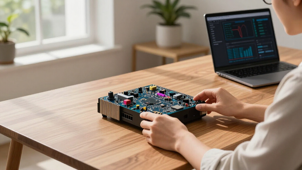
purpose-built AI chips for inference
As an affiliate, we earn on qualifying purchases.
As an affiliate, we earn on qualifying purchases.
Unclear Timeline for Widespread Adoption
While prototypes and small-scale deployments of specialized hardware are underway, it is not yet clear when these chips will become mainstream or how quickly existing infrastructure will transition. The pace of development depends on technological breakthroughs in low-voltage silicon, memory interconnects, and workload-specific design, which are still in progress. Additionally, the economic and supply chain impacts of this shift remain uncertain.
As an affiliate, we earn on qualifying purchases.
Next Steps in AI Hardware Development and Deployment
Industry leaders and hardware developers are expected to release new generations of inference-optimized chips within the next two to three years. These will likely feature integrated memory pools, low-voltage operation, and workload-specific architectures. Meanwhile, AI service providers and data centers will experiment with these new chips, gradually scaling their deployment as performance and cost benefits become evident. Monitoring these developments will be key to understanding how quickly the industry transitions away from general-purpose GPUs.
As an affiliate, we earn on qualifying purchases.
Key Questions
Why are current GPUs considered inefficient for AI inference?
Current GPUs are designed for general-purpose computing and have been retrofitted for AI inference. They are limited by thermal constraints, memory latency, and lack of workload-specific optimization, leading to lower utilization and higher power consumption for inference tasks.
What are the main advantages of purpose-built AI chips?
Purpose-built AI chips can operate at lower voltages, reduce thermal issues, optimize memory and interconnect architectures, and be designed specifically for inference workloads, resulting in higher throughput, lower costs, and better energy efficiency.
When might we see widespread adoption of specialized inference hardware?
Experts expect new hardware optimized for inference to emerge within the next two to three years, but full industry adoption will depend on technological, economic, and supply chain factors.
How will this shift impact AI service providers?
AI providers could benefit from lower operational costs, improved scalability, and increased capacity to serve billions of users and agents, enabling more widespread and affordable AI applications.
What remains the biggest challenge in developing specialized AI hardware?
The main challenges include achieving reliable low-voltage silicon, reducing memory latency at scale, and designing workload-specific architectures that can be manufactured cost-effectively at large scale.
Source: ThorstenMeyerAI.com
Fall Picks
fall essentials
As an affiliate, we earn on qualifying purchases.